Fermi Level In Semiconductor Formula : equilibrium-semiconductor - THE SEMICONDUCTOR IN EQUILIBRIUM CHARGE CARRIERS IN SEMICONDUCTOR In ... / So at absolute zero they pack into the.
Get link
Facebook
Twitter
Pinterest
Email
Other Apps
Fermi Level In Semiconductor Formula : equilibrium-semiconductor - THE SEMICONDUCTOR IN EQUILIBRIUM CHARGE CARRIERS IN SEMICONDUCTOR In ... / So at absolute zero they pack into the.. Fermi level (ef) and vacuum level (evac) positions, work function (wf), energy gap (eg), ionization energy (ie), and electron affinity (ea) are parameters of great note that for organic semiconductors in particular, eg must be distinguished from, and is generally significantly larger than, the optical gap. Related threads on fermi energy and fermi level in semiconductors. A key condition is charge neutrality: It is the widespread practice to refer to the chemical potential of a semiconductor as the fermi level, a somewhat unfortunate terminology. Each trivalent impurity creates a hole in the valence band and ready to accept an electron.
Uniform electric field on uniform sample 2. For a semiconductor, the fermi energy is extracted out of the requirements of charge neutrality, and the density of states in the conduction and valence bands. Related threads on fermi energy and fermi level in semiconductors. What is fermi level in semiconductor? The affinity rule does not always work well.
statistical mechanics - Does the Fermi level depend on temperature? - Physics Stack Exchange from i.stack.imgur.com It is a thermodynamic quantity usually denoted by µ or ef for brevity. Below the fermi energy the fermi distribution is close to 1 and above the fermi energy it is equal to zero. Www.studyleague.com 2 semiconductor fermilevel in intrinsic and extrinsic. Where −e is the electron charge. At 0 k all allowed energy levels in the valence band are filled by. Fermi level is the term used to describe the top of the collection of electron energy levels at absolute zero temperature. Semiconductor optoelectronics (farhan rana, cornell university). Note that all formulas derived for the forward bias case are also applicable to the reverse bias case.
What is fermi level in semiconductor?
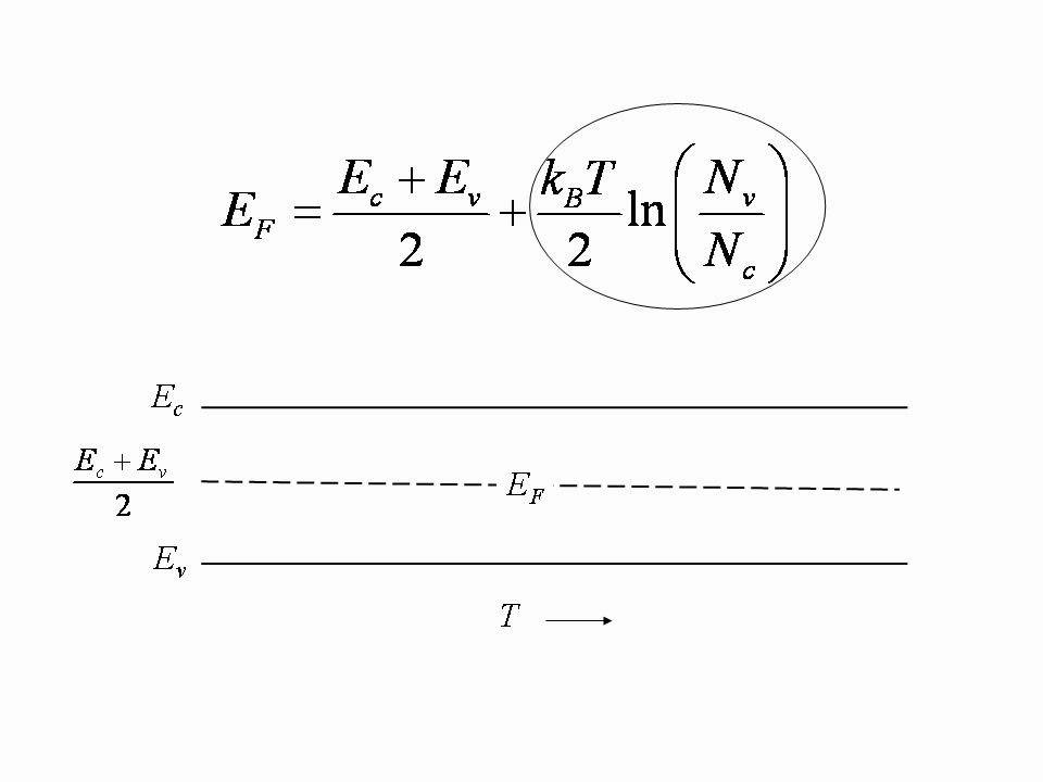
So fermi level lies in the middle of the conduction and valence band,that means inline with the forbidden energy gap. Also note that the fermi level in equilibrium is flat and constant throughout the device. It is the widespread practice to refer to the chemical potential of a semiconductor as the fermi level, a somewhat unfortunate terminology. Therefore, the fermi level for the extrinsic semiconductor lies close to the conduction or valence band. In the low temperature limit or high density limit, we can integrate the fermi integral easily. A substance for which the forbidden energy gap is relatively small than insulator. Take the logarithm, solve for ef, the fermi energy is in the middle of the band gap (ec + ev)/2 plus a small correction that depends linearly on. Related threads on fermi energy and fermi level in semiconductors. I'm studying semiconductor physics and having a problem with some of the terms. Ne = number of electrons in conduction band. Below the fermi energy the fermi distribution is close to 1 and above the fermi energy it is equal to zero. At 0 k all allowed energy levels in the valence band are filled by. We can find the intrinsic fermi level and simplify the results somewhat:
For a semiconductor, the fermi energy is extracted out of the requirements of charge neutrality, and the density of states in the conduction and valence bands. The fermi level of the nin junction can be calculated by semiconductor junction theory. Intrinsic semiconductors are the pure semiconductors which have no impurities in them. Ne = number of electrons in conduction band. At 0 k all allowed energy levels in the valence band are filled by.
Fermi Energy of an Intrinsic Semiconductor - YouTube from i.ytimg.com The fermi level does not include the work required to remove the electron from wherever it came from. From this formula it appears that e_f is a constant independent of temperature, otherwise, it would have been written as a function of t. A key condition is charge neutrality: Electrons are fermions and by the pauli exclusion principle cannot exist in identical energy states. Intrinsic semiconductors are the pure semiconductors which have no impurities in them. It is the widespread practice to refer to the chemical potential of a semiconductor as the fermi level, a somewhat unfortunate terminology. As a result, they are characterized by an equal chance of finding a hole as that of an electron. The dashed line represents the fermi level, and the.
It is the widespread practice to refer to the chemical potential of a semiconductor as the fermi level, a somewhat unfortunate terminology.
Charge carrier densities and fermi level in extrinsic semiconductors strongly depend on temperature and impurity density. At 0 k all allowed energy levels in the valence band are filled by. Also note that the fermi level in equilibrium is flat and constant throughout the device. Related threads on fermi energy and fermi level in semiconductors. Semiconductor optoelectronics (farhan rana, cornell university). Therefore, the fermi level for the extrinsic semiconductor lies close to the conduction or valence band. The affinity rule does not always work well. Electrons are fermions and by the pauli exclusion principle cannot exist in identical energy states. Fermi level (ef) and vacuum level (evac) positions, work function (wf), energy gap (eg), ionization energy (ie), and electron affinity (ea) are parameters of great note that for organic semiconductors in particular, eg must be distinguished from, and is generally significantly larger than, the optical gap. Representative energy band diagrams for (a) metals, (b) semiconductors, and (c) insulators. But then, there are the formulas for the intrinsic fermi levels at any temperature t > 0k. Of free electrons at room temperature.
So at absolute zero they pack into the. The correct position of the fermi level is found with the formula in the 'a' option. Also note that the fermi level in equilibrium is flat and constant throughout the device. Charge carrier densities and fermi level in extrinsic semiconductors strongly depend on temperature and impurity density. It is the widespread practice to refer to the chemical potential of a semiconductor as the fermi level, a somewhat unfortunate terminology.
Solved Problems: Semiconducting Materials from www.brainkart.com The fermi level of the nin junction can be calculated by semiconductor junction theory. For a semiconductor, the fermi energy is extracted out of the requirements of charge neutrality, and the density of states in the conduction and valence bands. What is fermi level in semiconductor? Let us define dimensionless units ηf and r. But then, there are the formulas for the intrinsic fermi levels Note that all formulas derived for the forward bias case are also applicable to the reverse bias case. An extrinsic semiconductor is a material with impurities introduced into its crystal lattice. Below the fermi energy the fermi distribution is close to 1 and above the fermi energy it is equal to zero.
What is fermi level in semiconductor?
The affinity rule does not always work well. An extrinsic semiconductor is a material with impurities introduced into its crystal lattice. at any temperature t > 0k. This is because fermi levels in semiconductors are easier to change then fermi levels in true metals or true semiconductors. If the fermi level is below the bottom of the conduction band, it is possible to use the simplified formula. I cant get the plot. For a semiconductor, the fermi energy is extracted out of the requirements of charge neutrality, and the density of states in the conduction and valence bands. Of free electrons at room temperature. Semiconductors are materials that possess the unique ability to control the flow of their charge carriers, making them valuable in applications like cell phones, computers, and tvs. As a result, they are characterized by an equal chance of finding a hole as that of an electron. Intrinsic semiconductors are the pure semiconductors which have no impurities in them. So at absolute zero they pack into the. Each trivalent impurity creates a hole in the valence band and ready to accept an electron.
To start with, we will first try to explain what a red card is, it's a reloadable debit card or often called a prepaid debit card which is given . The doordash red card is used to pay certain merchants for the food that is being purchased. You can pay for some doordash orders using the red card. The red card is a doordash driver's most valuable asset. It is used just like any other debit card. So....McDonald's is officially a Doordash partner now, I tried to place the order out of habit from preview.redd.it The red card is a doordash driver's most valuable asset. Doordash red card is a credit card that dasher uses to make payments for some doordash orders. *fast card numbers within 1 hour of purchase. Doordash red card is kind of a credit card that you can while driving for doordash. The doordash red card is used to pay cer
Malaysia Visa Invitation Letter / Ivisa Com In Review 2021 Is It Really Legit Important Update - Applicant is not required to be present when applying for invitation letter: . Failure to do so will seamen: Complete information regarding malaysia e visa online application process as well requirements and visa fee have been shared in this video. When inviting a person to your country. Bank statement / traveller's cheque. Visa requirements for malaysian citizens are administrative entry restrictions by the authorities of other states placed on citizens of malaysia. When inviting a person to your country. Malaysia offers 3 types of visas for tourism purpose. A visa invitation (also referred to as a tourist voucher, visa support, invitation, visa invitation or invitation letter) is the main document which is when ordering a visa support/invitation through us, you do not need to send any original documents. For a single entry visa, maximum validity is only 30 days. Doc
The Crew Board Game : The Crew Quest For Planet Nine Card Game Kennerspiel Des Jahres Winner Cooperative Space Adventure 2 To 5 Players Ages 10 And Up Trick Taking 50 Levels Of Difficulty Endless Replay Toys Games Amazon Com : During each mission, it is not the amount of tricks, but the right tricks at the right time. . In order to meet the various challenges, communication will be essential within the team. See more of the crew on facebook. The quest for planet nine. But in space it will be more difficult than expected. But you will only succeed if you can work together as a team. Boardgame brody loves bringing his old love of trick taking and adding a modern twist in the crew: Find the best deal for the board game the crew: At the start of a mission, all cards are dealt to the players and whoever has the 4 rocket is 'the captain'. It's time to explore the united states! Baiam or kuala), you embody a character in an immersive story in which your choices


Comments
Post a Comment